 wire
wireExamples
Each example below is a complete, valid Wire Lang document you can
copy and render with wire render file.wire --out file.svg.
The diagrams shown are the actual SVG output of Wire Lang's
deterministic renderer. Read the
syntax reference if any statement is
unfamiliar.
LED current limiter
A 5 V battery drives a red LED through a 220 ohm current-limiting resistor — the canonical first circuit.
schematic
  title "LED current limiting circuit"
  description "A 5V battery drives a red LED through a 220 ohm resistor."

  component BT1 Battery voltage=5V
  component R1 Resistor value=220ohm
  component D1 LED color=red

  net VCC: BT1.+, R1.1
  connect R1.2, D1.A
  net GND: D1.C, BT1.-

  annotation "Current limiting resistor" near R1
  render direction=left-to-right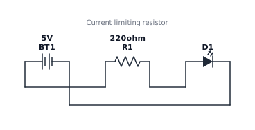
RC low-pass filter
A first-order RC low-pass filter between a header input and output.
The Header component exposes the pins listed in
pins=[...] as terminals.
schematic
  title "RC low-pass filter"
  description "A first-order RC low-pass filter between a header input and output."

  component J1 Header pins=[IN,OUT,GND]
  component R1 Resistor value=1k
  component C1 Capacitor capacitance=100nF

  net IN: J1.IN, R1.1
  net OUT: R1.2, C1.1, J1.OUT
  net GND: C1.2, J1.GND

  annotation "Cutoff ~1.6 kHz" near net OUT
  render direction=left-to-right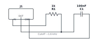
Soil sensor module
A locally defined module-style component (SoilSensor)
wired to a header and a pull-down resistor. This shows
define component ... end with symbol module,
drawn with the bus-rail layout mode.
schematic
  title "Soil sensor input"
  description "A local soil-sensor module wired to a header and a pull-down resistor."

  define component SoilSensor
    terminal VCC
    terminal GND
    terminal AOUT
    symbol module
  end

  component S1 SoilSensor
  component R1 Resistor value=10k
  component J1 Header pins=[VCC,GND,A0]

  net VCC: J1.VCC, S1.VCC, R1.1
  net GND: J1.GND, S1.GND
  net SENSOR: S1.AOUT, R1.2, J1.A0

  render layout=bus-rail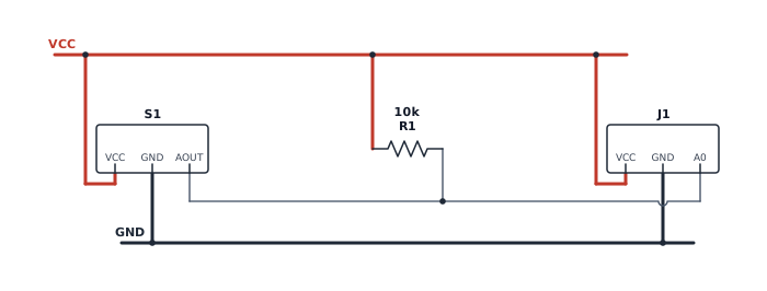
NPN LED driver
An NPN transistor switches a green LED from a 9 V supply, driven
through a base resistor. Transistor terminals are
C (collector), B (base), and
E (emitter).
schematic
  title "NPN LED driver"
  description "An NPN transistor switches a green LED from a 9V supply, driven through a base resistor."

  component BT1 Battery voltage=9V
  component R1 Resistor value=1k
  component R2 Resistor value=330ohm
  component Q1 NPNTransistor
  component D1 LED color=green
  component J1 Header pins=[IN,GND]
  component G1 GroundReference

  net VCC: BT1.+, R2.1
  net LEDK: R2.2, D1.A
  connect D1.C, Q1.C
  net BASE: J1.IN, R1.1
  connect R1.2, Q1.B
  net GND: Q1.E, BT1.-, J1.GND, G1.GND

  annotation "Base current limit" near R1
  render direction=left-to-right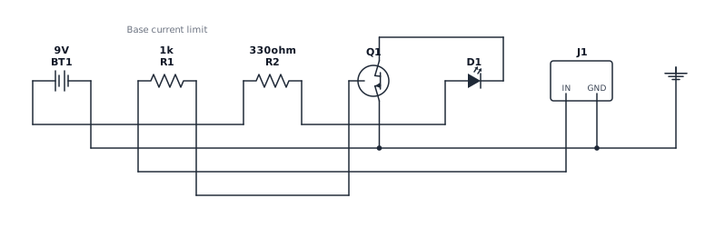
Battery LED with push button
A 3 V battery lights a red LED through a current-limiting
resistor when a push button is pressed. Demonstrates
PushButton and multiple annotations.
schematic
  title "Battery LED with push button"
  description "A 3V battery lights a red LED through a current-limiting resistor when the push button is pressed."

  component BT1 Battery voltage=3V
  component SW1 PushButton normally=open
  component R1 Resistor value=220ohm
  component D1 LED color=red

  net VCC: BT1.+, SW1.1
  connect SW1.2, R1.1
  connect R1.2, D1.A
  net GND: D1.C, BT1.-

  annotation "Press to light the LED" near SW1
  annotation "Current-limiting resistor" near R1
  render direction=left-to-right
Standard symbol coverage
A switched 9 V rail feeds an RLC network, a PNP low-side driver, and an amber LED, with a filtered output header. This "kitchen sink" exercises the core standard symbols in one schematic.
schematic
  title "Switched RLC bench demo"
  description "A switched 9V rail feeds an RLC network, a PNP low-side driver and an amber LED, with a filtered output header. Exercises a selection of standard symbols."

  component BT1 Battery voltage=9V
  component SW1 SPSTSwitch state=closed
  component BTN1 PushButton normally=open
  component L1 Inductor inductance=10mH
  component D1 Diode
  component R1 Resistor value=1k
  component R2 Resistor value=4k7
  component C1 Capacitor capacitance=100nF
  component C2 PolarizedCapacitor capacitance=10uF
  component Q1 PNPTransistor
  component D2 LED color=amber
  component J1 Header pins=[VBUS,SIG,GND]
  component G1 GroundReference

  net VIN: BT1.+, SW1.1, BTN1.1
  net RAIL: SW1.2, BTN1.2, L1.1, R1.1, C2.+, J1.VBUS
  net MID: L1.2, D1.A, R2.1, Q1.E
  connect D1.C, C1.1, Q1.B
  net SIG: R2.2, C1.2, Q1.C, D2.A, J1.SIG
  net GND: BT1.-, R1.2, C2.-, D2.C, J1.GND, G1.GND

  annotation "PNP low-side driver" near Q1
  annotation "Output filter" near net SIG
  render direction=left-to-right
Bus-rail block diagram
A sensor and LED driver around an MCU hub, drawn with
render layout=bus-rail: a top supply rail, a bottom
ground rail, an I²C bus bundled into a trunk, color-coded control
lines, and a button and LED placed automatically next to the pins
that feed them. It also shows the built-in IC type with
numbered, named pins.
schematic
  title "Bus-rail layout demo"
  description "A sensor and LED driver around an MCU hub, drawn with top and bottom rails, a bundled sensor bus, colored control lines, and a button in the control band."

  component U1 IC pins=[1:VCC@left, 2:GND@left, 3:SCL@right, 4:SDA@right, 5:INT@right]
  component U2 IC pins=[1:3V3@left, 2:GND@left, 3:SCL@left, 4:SDA@left, 5:IRQ@left, 6:BTN@left, 7:DRIVE@right, 8:FAULT@right]
  component U3 IC pins=[1:VIN@left, 2:GND@left, 3:IN@left, 4:FAULT@left, 5:OUT@right]
  component SW1 PushButton
  component D1 LED color=green

  net VCC: U1.VCC, U2.3V3, U3.VIN
  net GND: U1.GND, U2.GND, U3.GND, SW1.2, D1.C
  net SCL: U1.SCL, U2.SCL
  net SDA: U1.SDA, U2.SDA
  net INT: U1.INT, U2.IRQ
  net DRIVE: U2.DRIVE, U3.IN
  net FAULT: U3.FAULT, U2.FAULT
  net BTN: SW1.1, U2.BTN
  net LED_OUT: U3.OUT, D1.A

  render layout=bus-rail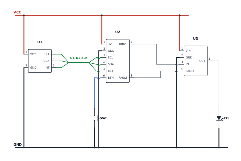
More example sources live in the examples/ directory of the repository.